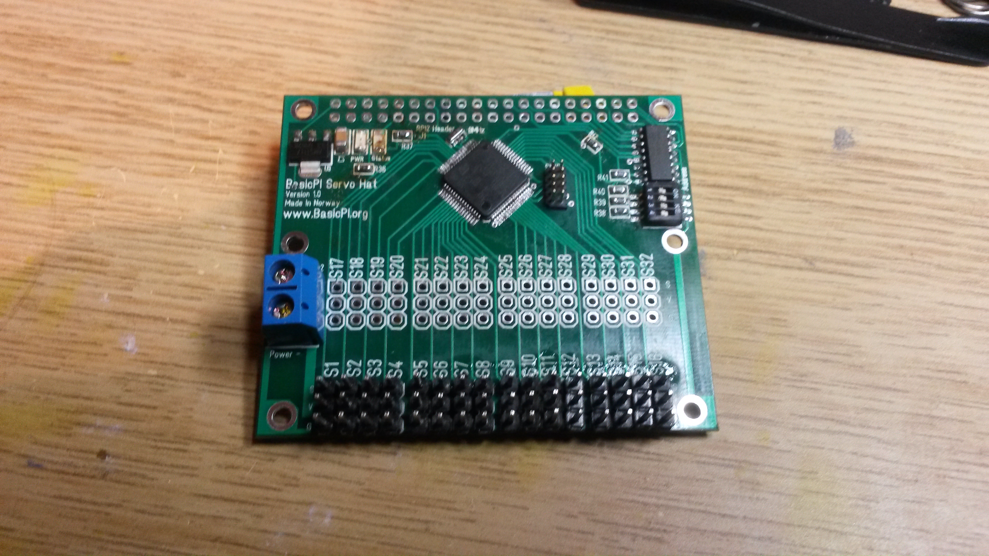
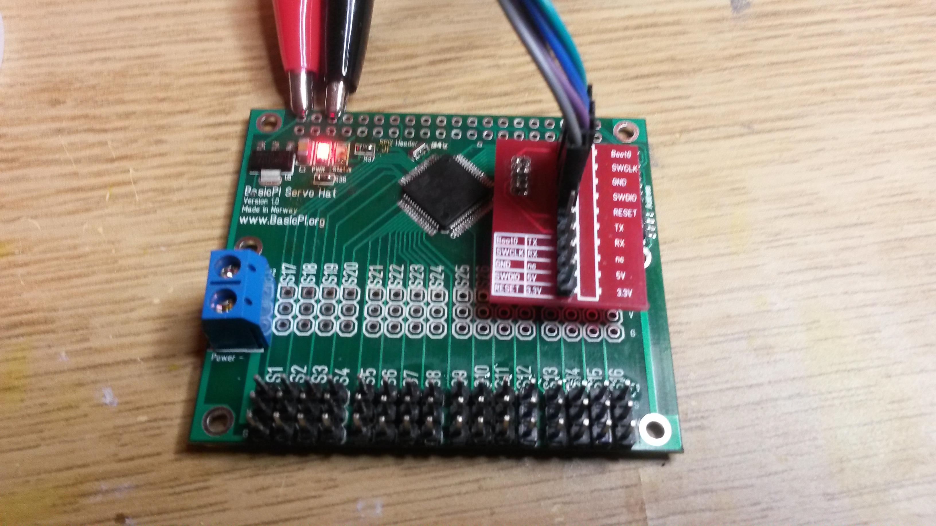
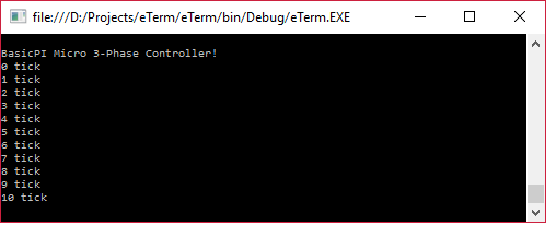
Finally had the time to assemble a 32 x Servo Hat. Have not written any code for it yet, but always nice to see SWD answering and led’s coming up with a 10mA current on the lab psu – Things look normal. Will get down to wrapping up a servo controller and assembling a RPI with an user interface later. I will be using RPI3 because of it’s build in Wifi to control my robot.
The MCU on this is STM32F105RB, so it got plenty of juice and IO. Controlling Servos and motors are obvious, the channels can also be used for digital I/O and analogue I/O.
The picture above show the SWD adapter connected and illustrate why I need to modify this to go out as a thin board horizontally. I only mounted channel 1-16 for now due to the space conflict with the adapter.
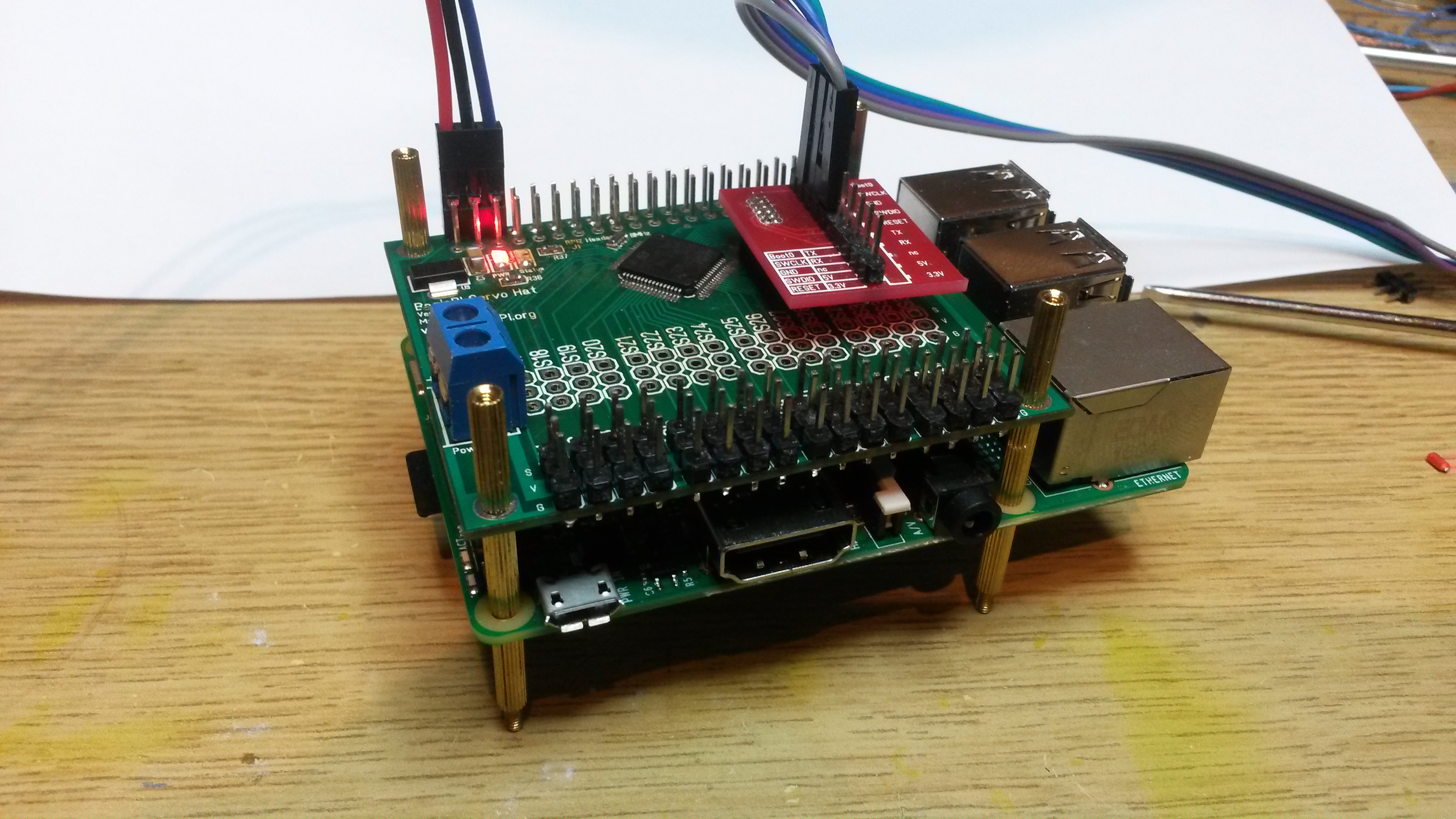
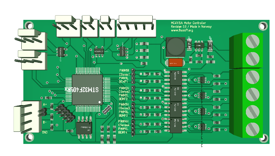
This last picture show the 32xServo mounted on Raspberry PI 3. It can be stacked with an extra spacer or by mounting it at top. If stacked you can control 8 x 32 = 256 servos. More interesting is probably the capability to combine Hat’s to make Advanced systems.
