Lab PSU 0-30V /10A – Part 13

Right now I am waiting on heat sink material so we can start testing the regulator with 5-10A continuous. I have done a few tests without and managed to burn transistors. My small fan’s do help a lot, so I expect a combination of heat sinks and fan’t to do Wonders.

Heat dissipation is the Achilles of this old linear regulator but, I just fancied doing this old design before I start on a more modern, digital PSU. The advantage of this design is low noise – or at least should be.

I had some challenges with the current regulator, but finally realised reading up on the issue that voltage between pin 2 & 3 on LM723 need to be ca 0,62V before it start working. This means I probably need to consider using a relay to switch current range between shunts for 5A & 10A because shunts designed for 10A will have little impact in the lower area. I will return to this as soon as I get the heat sink and fan’s mounted properly.

The blue metal box I purchased (below) is ok. For 17.- USD this is good value, but it is a bit small for what I want to do. I probably need more space due to heat dissipation at 10A, but we will see – I actually ordered more of these boxes due to their good value.

Something else that is very clear is that I need to mount temperature sensors and activate overheating logic by cutting output if the transistors overheat.

PLC – Ethernet Module 2

Looks like the GSM module will be added to the Ethernet Module. Found several modules in price from 1.27 to 4 USD. Basically UART operated with support of GSM + GPRS, TCP/IP, UDP/IP, SMS etc. The cheapest kit is data only, but some of the others include voice as well. More important is that datasheets and programming guides are available.

M590E
SIM800C
A6

The M590E is SMS/Data only and cost 1.27 USD, the others include voice and cost 3-4 USD. More expensive modules with 3G/4G etc exist, but GSM/GPRS should be sufficient. GPRS have a bandwidth of ca 85Kbps.

I need to find space for these modules + SIM Card and antenna, but I think that is very doable. It is also an option to use one of the breakout boards “as is”.

PLC – Ethernet Module

The block diagram above show the Ethernet module. Starting with a dual RS-X to the backbone and a SPI based W5500 for Ethernet connectivity. In addition we add a ESP-12 for Wifi, SPI Flash for storage and a RTC battery & oscillator as well as the mandatory SWD connector. I hope to have a 3D model of this board ready within the next days. The red box on Ethernet/Wifi mark that this is galvanic isolated.

The STM32 design will differ from earlier designs as I will be using x-tal’s with higher quality and add the RTC x-tal as well. I am toying with the idea of testing a supercap as “battery”. A normal battery has a degrading over time that forces it to be replaced on regular basis. As a RTC battery only need to survive a power down for some time it could be interesting testing a supercap as an option. It is also an option to dedicate one of the available pin’s on the backbone to “Power off battery” and use wakeup functionality on the MCU.

I have also drafted a GSM as optional add-on here. As this will be an external breakout it might make sense to add it to this module rather than creating a separate one. This is however something I need to look into. At present I have little experience using GSM like this.

The RS-X backbone speed will probably be 2.5Mbps, both lower and higher speeds are an option.

PLC – All In One Home Central

A Modular PLC system will have some size & cost, and as a home central should be small, easy to hide and low cost it might be wise to produce a specialized “All In One” solution. The diagram above illustrate the content with “backbone” replaced by a MCU. The C firmware will basically only be a simplified version of what we use on the modular system. The content focus on communication only since we expect distributed nodes communicating through RS-X to perform the sensor/actuator parts.

PLC Backbone Block Diagram

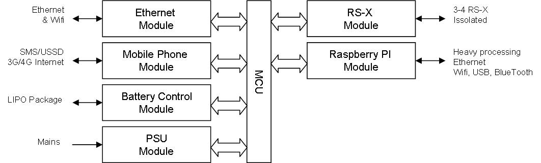
Using STM32F405RG on everything is an overkill, but I can always consider dropping down to STM32F105RB/C later. This M4 gives us a powerfully MCU on each module capable of truly distributed processing as we are promoting in Plain.

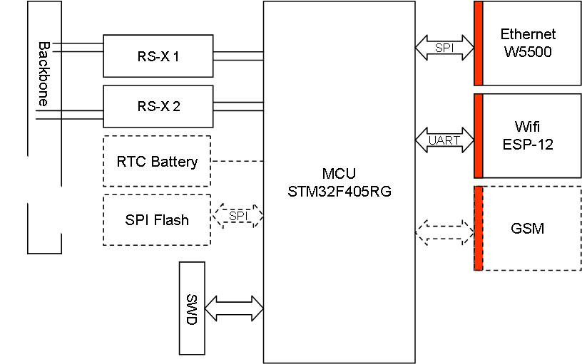
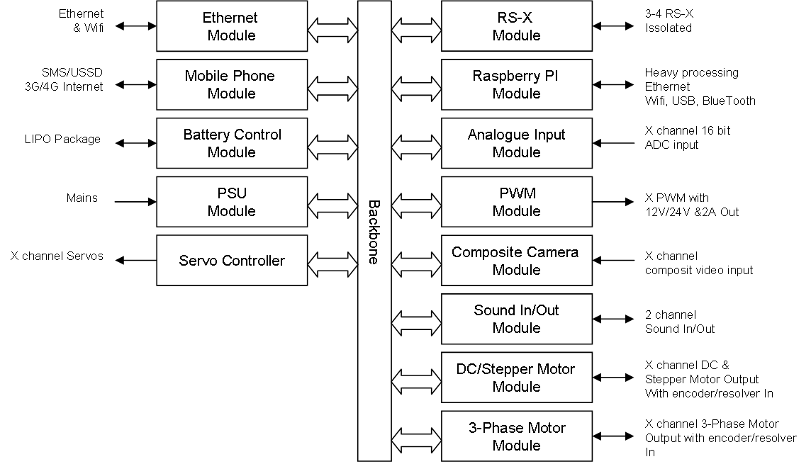
Ethernet Module is what I have started on now. This will host a STM32F405RG, 2 RS-485’s for the backbone, a W5500 based Ethernet and optionally a ESP-12 module for wireless. I am also adding RTC battery, SPI flash and a SWD connector. I need to see what space I have available, but as with my previous Raspberry PI Hat’s I intend to re-use much of the MCU related design on every Board if pins & space allow it.

RS-X Module connect the 2 backbone lines to 3-4 isolated network lines. I want isolation on anything in & out of the PLC.

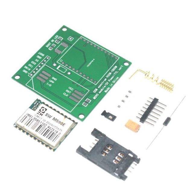
Mobile Phone module is for internet connectivity on remote places or as a secondary backup should a primary internet be cut. It exist so many small, low cost modules these days that we just grab one of those.

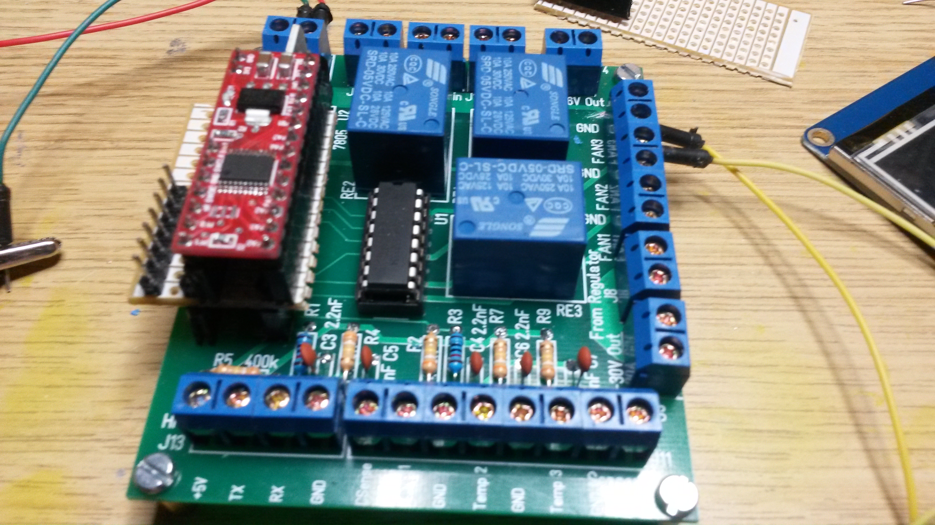
Battery Control Module is so we can connect a LIPO package to operate if mains fall out. This should also include charging and monitoring of the battery.

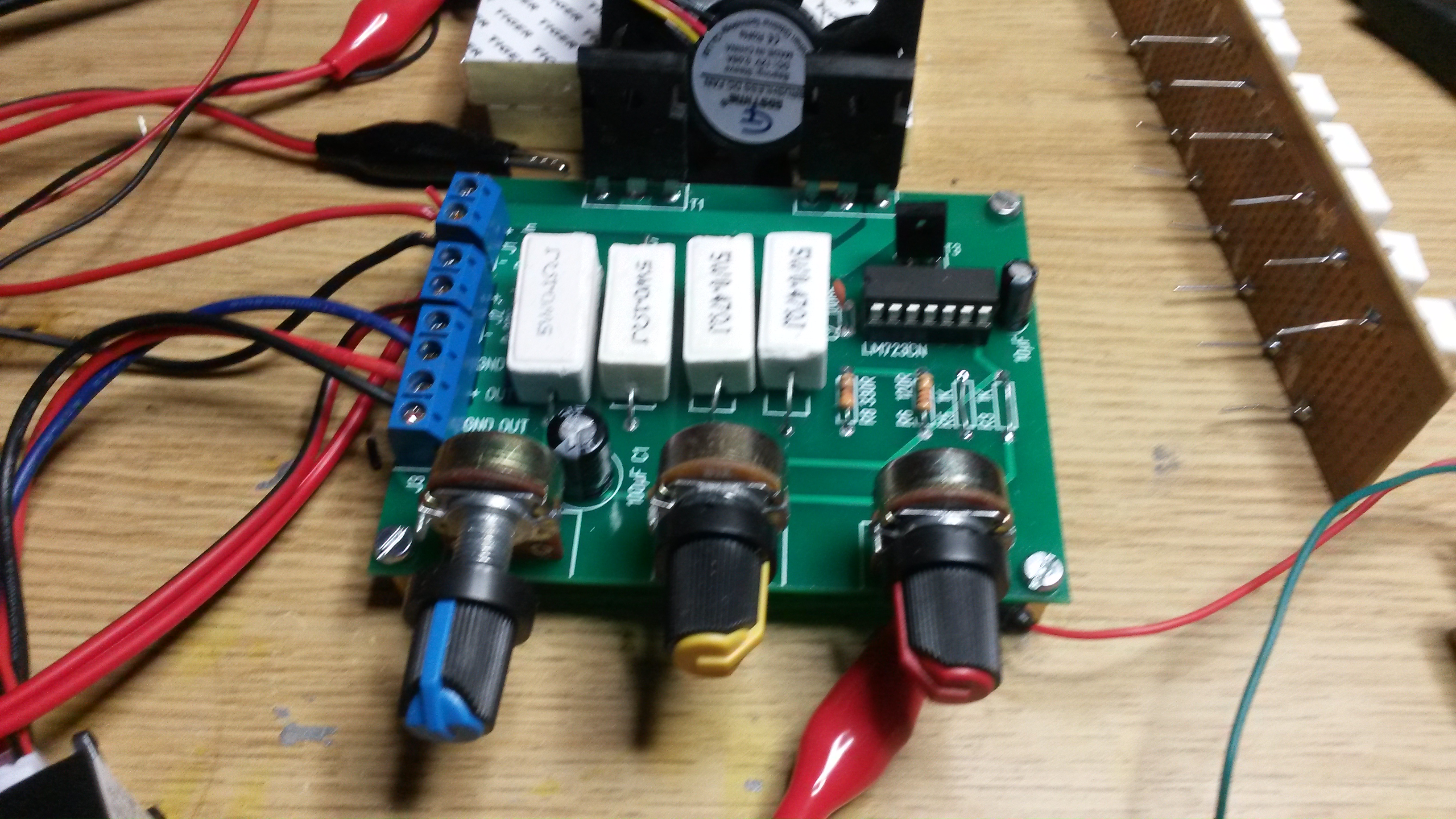
PSU Mains Module is basically PSU modules needed for 5V, 12V, 24V &48V.

Raspberry PI Module will allow us to interconnect with a Raspberry PI for computing, Ethernet, Wifi, USB, Bluetooth etc. The target here is Raspberry PI 2, 3 or Zero W.

Analogue Input Module is a x channel 16 or 24 bit ADC input module. This allow us to read analogue sensors with some accuracy. We need more than the internal 12 bit ADC, so I am thinking maybe a low cost 12 bit board and a bit more expensive 24bit board.

PWM Module is a x channel PWM output, each channel formed as a Half H-Bridge and supporting 2A continuous current. We probably should manage 8 channels – not shure.

Composite Camera Module. I am not sure about this board as I am tempted to use H.264 camera’s only in which case I will ditch this module.

Sound In/Out Module is basically targeting doorbell, but I am open for the possibility to provide a multi-channel music mixer as well. I need to consult with friends in the London music industry a bit, and it is possible this actually will be several boards to adapt to a stage show.

DC/Stepper Module will basically be very similar to the PWM module, but I probably need various currents & voltages for different motors. I am thinking only of small motors supported directly because I expect separate controllers for the larger motors.

3-Phase Motor controller – well, the name say it all, but I am not sure I want to make this board. The reason is because a 3-phase motor usually require some power that is better handled on a separate controller on the other side of an isolated RS-X. Let’s see…

Servo Controller is probably a 16 channel controller like we created before on a Hat, but I will be using Timer’s for PWM this time to get a 16-bit resolution on the PWM duty out.

As mentioned a few times before – this is an idea draft and I write it down to let it mature – plans will change.

PLC Module – Mechanic scetch

I am toying with using my 3D printer to (1) print a module box and (2) to print PCB holders as illustrated above. This was an early draft – the idea is that you push the module in and use a screwdriver to mount it – I need to look for low cost alternatives here and have a concept before I order the backbone.

New Micro PLC Backbone

My previous backbone board had to little space between connectors + no connection for PSU & communication – this one has 10mm between connectors which is more realistic – thought I still expect one Add-On board to use ca 20mm width. The total width “as is” is 100mm, so it is still very small.

I actually need to find a solution on the mechanical boxing before I finish this one + this is still only an idea draft that need to mature. I probably should add bias and terminator for RS485 on the backbone. Have some spare space on right.

As for add-on boards I am toying around with the following ideas;

  • An Ethernet connectivity board.
  • An RS-X connectivity board.
  • An Raspberry PI connectivity board.
  • An analogue input board.
  • A PWM channel board.
  • A camera input board.
  • A voice & mic board.
  • A DC-/Stepper- Motor board.
  • A 3-Phase motor board.
  • A GSM/3G/4G Board.

We can have a lot of fun here, but I will let these ideas mature a bit…

SMD versus Hole Through

This came as a surprise to me – it is only 1,5 years ago I started doing SMD electronics. My previous experience had only been hole through technology. But, as hole through have so many limitations I decided to jump in and give it a try – the first component I tried was a LQFP48 – a STM32F103CB. After watching some Youtube movies I picked up a trick and soldered it with an ordinary soldering iron – it worked. I started with 1205 components, but won’t use anything larger than 0603 these days.

As I now do a hole through project it serve to remind me of how much easier it is to work with SMD than hole through:

  • To solder a hole through you need to hold the PCB up-side down struggling with components falling off.
  • You have the same issue as you remove them.
  • Components that are easy to remove with Hot air on SMD is a paint on hole through.
  • The largest surprise was however in the EDA – your selection of components and technology is suddenly very limited.

The one advantage that Hole Through have is that things are larger and more people feel comfortable working on it – SMD do require some practice to get right, but it is seriously worth mastering. In sum – SMD is much easier to solder and work with than Hole Through IMO.

Lab PSU 0-30V /10A – Part 12

The good thing about a blog is that it is excellent for notes – if I make my work-notes here they are called “documentation” 🙂

The following are programming notes for the PSU Control Board:

PA10 – GPIO J1-4 Relay 1 – Connect extra 12V – 36V If Relay 2 is On.
PA9 – GPIO J1-5 Relay 2 – Connect extra 12V – 24V
PB1 – GPIO J1-6 Relay 3 – Switch On/Off Output from regulator.
PA7 – ADC J1-7 Temperature 3
PA6 – ADC J1-8 Temperature 2
PA5 – ADC J1-9 Temperature 1
PA4 – GPIO J1-10 Fan 3
PA3 – UART1 J1-11 RX
PA2 – UART1 J1-12 TX
PA1 – ADC J1-13 V Out. Measure Out Voltage in a split 10:1
PA0 – ADC J1-14 CSense Out. Measure Voltage in a split 10:1 before current shunt. CSense – V Out = shunt voltage.

Current Out = Shunt Voltage / (0.47R / 2)

PF0 – GPIO J2-6 Fan 2
PF1 – GPIO J2-7 Fan 1

Note 1: A 12 bit ADC scaled for 30V (30/4096) will detect ca 7mV changes in voltage drop over the shunt. Given a shunt resistor of 0.235 Ohm (0.007V / 0.235R) that gives a resolution on ca 31mA on the current calculations. This is a little less than I hoped for, but the alternative is to use an external current sensor to increase accuracy – I need to work on this a bit.

Lab PSU 0-30V /10A – Part 11

This pic shows my analogue regulator. You can see the 2 transistors and a fan in the back and my DIY load array on top left. I am actually quite happy with this after I mounted it on a proper PSU source in. The only things left is to get the current regulator working, but I am a bit handicapped in testing before I get a proper heatsink mounted. I have so far only tested 5A for a short period and had to abort as transistors started to overheat.

This shows my Control board. I have done more mistakes on this than I like to admit. The red PCB on left is the MCU – had to mount an adapter to allow for SWD connection so I can program it. Will start working on this a bit later. From my previous test I notice that the analogue regulator need ca 4V to work on, so I need to connect the 2nd PSU at 8V and the 3rd at ca 20V.

A few things to work on:

  • Need to get current regulator working.
  • Need to verify 10A continuous.
  • Connected GND rather than 12V on FAN output’s.
  • Forgot pull-up’s into ULN 2003 so relay’s hit in at random before MCU take control.