New 3D Printer

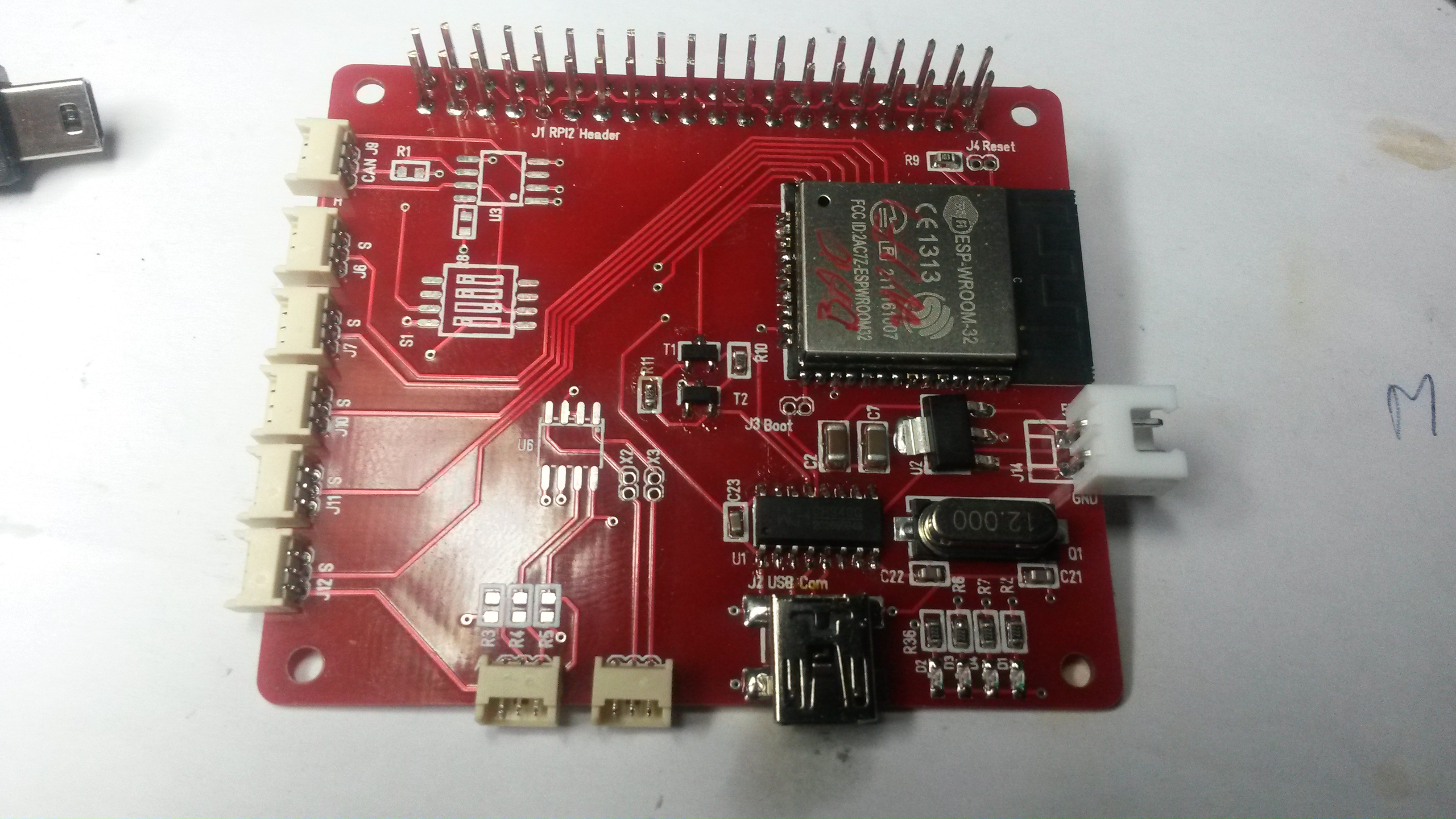
I do at present have 8 PCB’s + 3 designs I have not ordered yet in my modular control system, so I have a far to large backlog of electronics that need testing and code. The difference with my last 12 x PWM Hat is however that it target a project – my upgraded 3D printer.

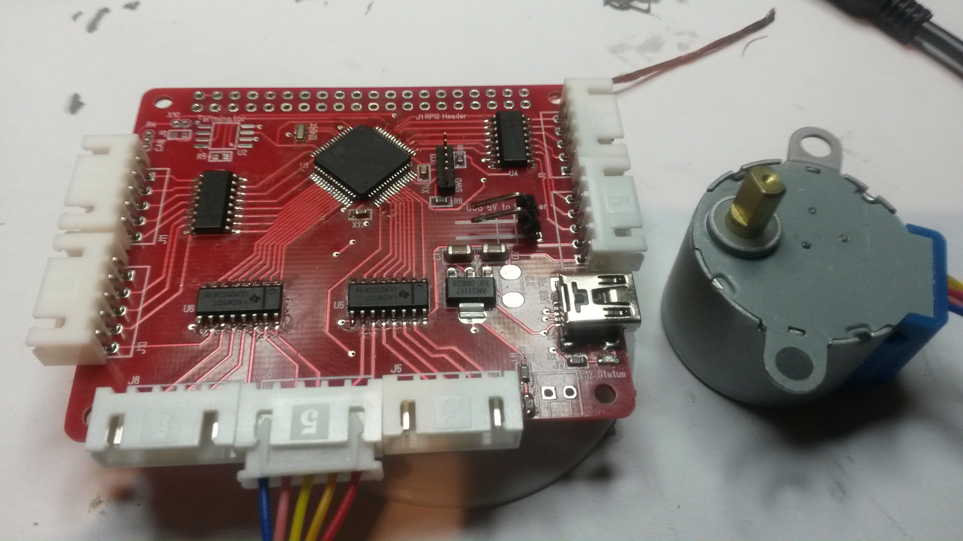
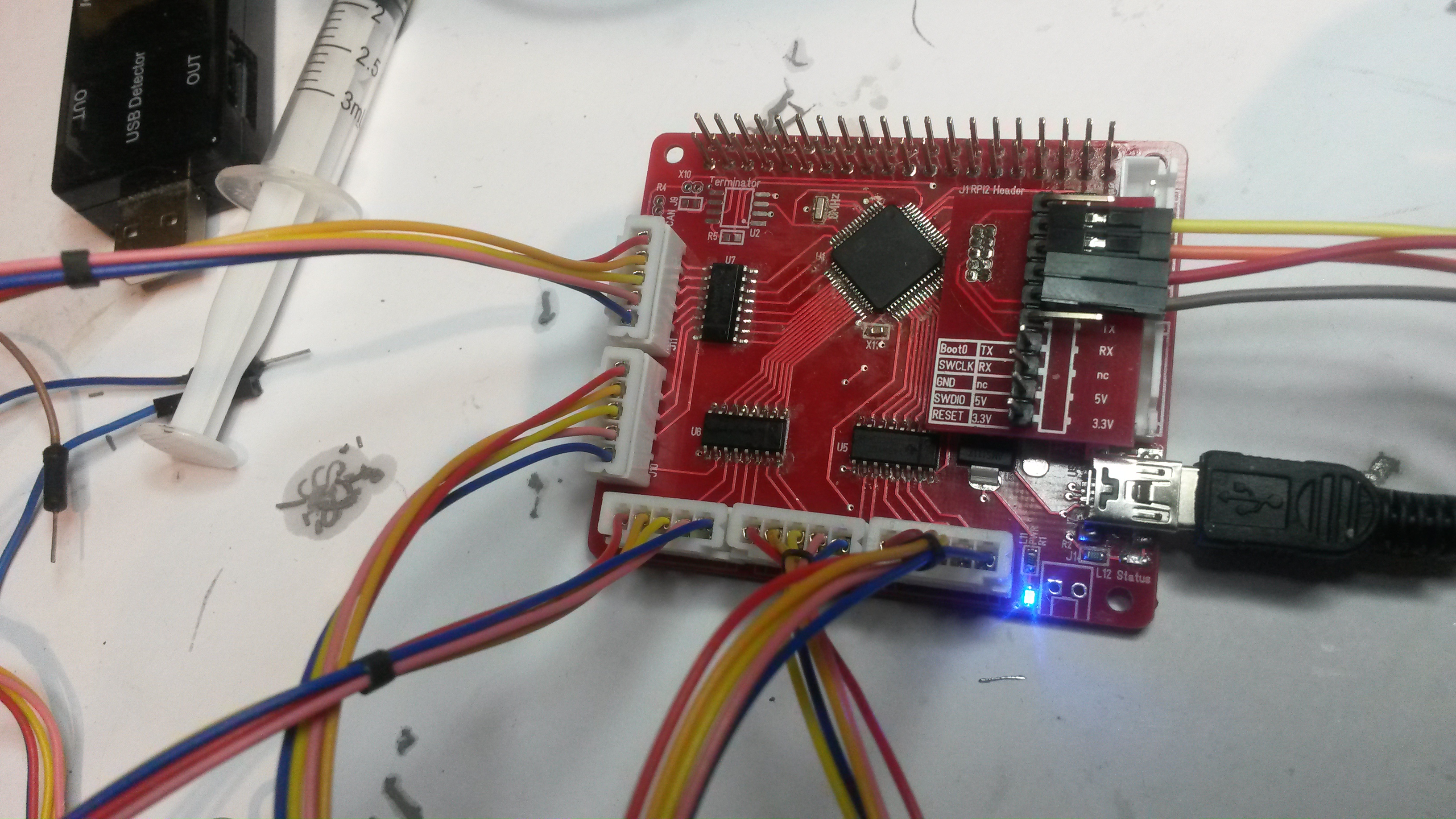
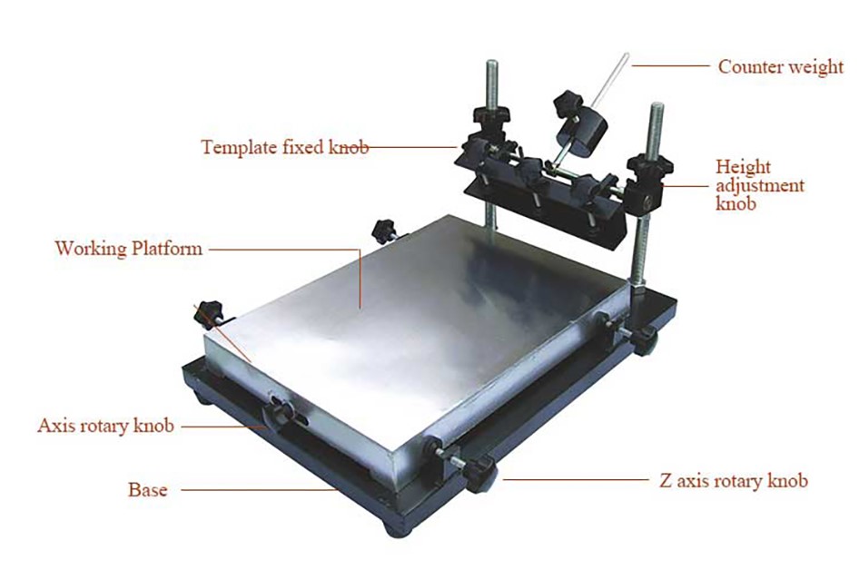
I purchased a Prusa i3 which basically is a clone of a generation 1 design and I want to use my modular control system on this one. I actually have 3 Arduino based control systems of which 2 used a fake FTDI chip that caused problems. But, I want to add features not available in the old control system.

Multi-material support means more than one extruder. This is mostly a mechanical re-design, but I need extra Stepper motor controller and logic to handle it.

Automatic calibration. Those of you who have used an early version of a 3D printer know how much work that goes into calibrating and ensuring that the printer is correctly configurated. This can be done automated by sensing the tilting of the plate using a “Z-Sensor”.

Torque based end-stops means that I do not use end-stop sensors, but sense current increase as the CNC machinery hit mechanical stoppers. This is goodbye to a lot of problems and wiring.

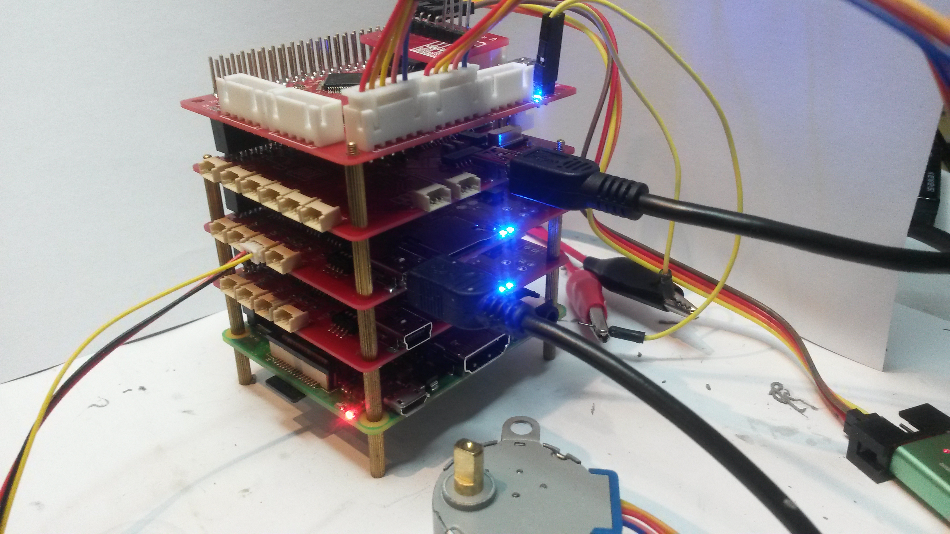
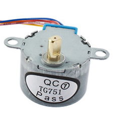
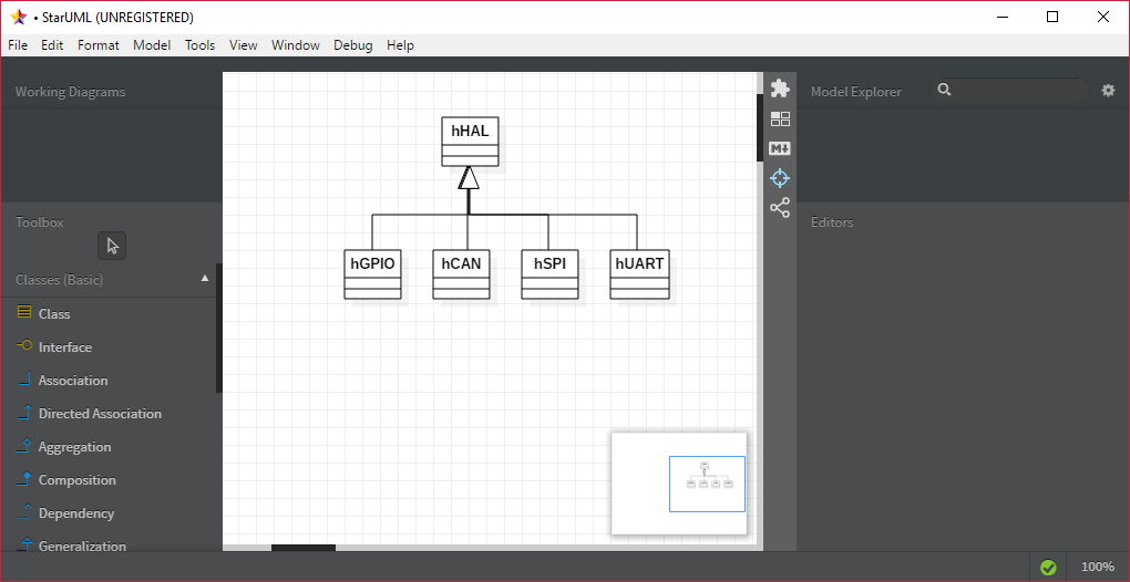
In the illustration above I assume I will use 5 modules to make a modular control system. One Wifi module that can be Raspberry PI or ESP32 based, a XPortHub to access USB, MMC and HMI. MMC can be used to spool jobs. A 12 X PWM used as 4xStepper to control X,Y and 2xZ Steppers. A 2nd 12 x PWM to control 2 x Extruder feeders and 3 x temperature heaters for heatbed and extruders, and finally a 32 x IO to get temperature sensors and a Z-distance sensor. This is just an early illustration.

The Z-distance sensor I want to use is a small laser that can sense the distance from Extruder to the plate. This can during calibration sense the tilting of the base plate and adjust G-Code parameters so it get correct.

This is an excellent test bed for my modular control system. It is so many excellent All-In-One systems for 3D Printers and my favorite is the new MK3 from Josef Prusa so we could have done this much easier. But, I need a test bed and this is an excellent start to drive development.

High Side Current Sensor

I decided to Change the 12 x PWM Hat to use High Side Current Sensors. Below is the schematics of the new sensors. This means I measure current out on each PWM signal.

Using high side sensors actually simplified the routing so it was a straight forward change. The reason I started with low side sensors is because that is straight forward for DRV8313 and more common for 3-phase. It would have been ok for Stepper and DC motors, but it made it difficult to measure current if you used a single PWM channel stand-alone.

12 x PWM Hat

 This 12 x PWM Hat have 12 x high side current sensors. The PWM driver have a separate PSU, DRV8313 is rated 60V and INA194 is rated -16 to 80V so they are not that easy to break giving the Hat a very decent protection level. A separate TVS and capacitor bank on motor PSU will in addition suppress unexpected spikes + there will be larger protection on the PSU itself. I feel quite comfortable with this design, but testing will show.

Connecting the current sensors low side is not the most optional for individual PWM signals, but it is ok for 3-Phase and Stepper Motors where I wanted them the most. The challenge with PWM is that current mostly leave high side out and get connected to ground, meaning we never pass a current sensor on low side. But – again – I do have a SW trick that I will test. Adding these low side was most straight forward due to DRV8313. But, I will actually evaluate if I should move them high side. This would actually simplify the PCB – I think.

I am looking forward to work with this one due to the advanced functionality you get with current sensors – and if anyone wonder the first project is actually my 3D printer. I will write a separate article about that later.

3-Phase/Stepper/RPM Hat

This Hat was actually a challenge to route, but I managed it at the 4th attempt. I am quite happy with the result as well.

  • Raspberry PI Hat Format
  • STM32F405RG MCU, 32bit ARM M4, 168Mhz, 1Mb Flash, 196Kb SRAM.
  • 42Mbps backbone network. ca 30Mbps With Raspberry PI.
  • CAN Network
  • USB
  • Separate PSU for PWM
  • 12 x separate PWM signals, ca 1A each.
  • 3 x Stepper Motors 2,5A
  • 4 x 3-Phase Motors 2.5A
  • 6 x DC Motors.
  • 24V design capable to support 48V with some cap/diode changes.
  • 24 connector terminal block with 12 signals and 12 ground connections.
  • 12 separate current sensors.
  • 12 separate Half H-Bridges allowing a very flexible usage.
  • Based on DRV8313 3 x Half H-Bridge Driver.

I have many designs, but the flexibility of this one is in a category of itself.

  • Gimball controller
  • CNC/3D Printer controller
  • Running DC Motors/PWM signal up to 10A by combining ports.

I must also admit that it feels good to be finish with this after so many failures on routing this very design. I have done many weighted compromises here, so I will need the MCU on this one, but it will be fun!

My motivation to do this one is that it is a key component in a very special control system where it is possible to actually earn some money. But, well – I can’t tell every secret in here 🙂

PWM Noise

The 2 blue signals crossing the bigger, red Power lane is asking for trouble. The blue lanes are 0-3V ADC signals, while the power lane is feeding PWM MOSFET’s. What will happen is that PWM noise from current spikes will jump over to ADC signals and create a false current signature.

But, I believe it is to my advantage that I have a fast MCU and no electronic filtering, meaning I can apply smart filtering in SW using the high sampling frequencies available on the ADC. Well, we will see. But, I have promissed myself that I will look into 4-layer PCB designers after this one.

MCU Factory Rejects

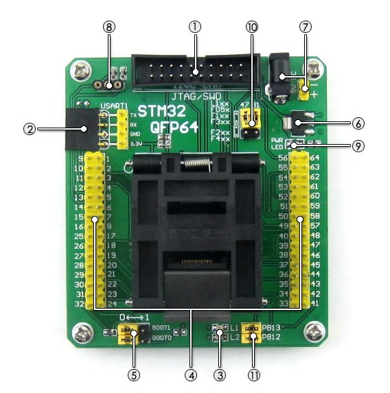
I must admit that sourcing for STM32F405RG is an issue. I have bought batches from China and I am rejecting a lot of MCU’s. The worst is actually the time to solder them on before I can test, so I seriously need the tester shown in my last article.

This is worst as I like now deal with a new board. I have soldered on 3 different MCU’s that all show up with failing memory sectors, and it’s a lot of stress on the PCB so you can only solder on/off so many times. After 3 fails on a new PCB I also start questioning other possibilities – do I as an example have a bad SWD on this board? SWD is a bit sensitive so if you have a bad SWD connector it might show up in various forms.

I managed to find a good tester for 44.- USD, so I am looking forward to that one. As much as I would like to test new boards I don’t want to waste more time on MCU unsecurity, so I will wait for the tester. I want to know that my MCU is good before I put it on.

I do however still need to sort out sourcing for STM32F405RG because this is unacceptable. But, with a tester I can actually test the batches I receive and slam down on bad sellers instantly to get my money back. I don’t expect the MCU’s to be perfect, but I expect them to work. This is prototyping and you can’t use my sources in production. But, I am getting rather pissed of with fraud schemes of selling factory rejects through Aliexpress! STM32F405 is specially bad for some reason.

I do however see that Farnell/Element14 sell this MCU for ca 9.- USD each in quantity of 10 delivered “next day” inside Norway – it is 2x my current cost, but it is tempting because of the time I waste on this.

Current Sensor Math

I currently plan using INA194 that have a 50x gain. As our max voltage in is 3.3V this means the max voltage over the shunt need to be 3.3/50= 66mV. Given a max current of 2.5A that gives a Shunt resistor R = V/A = 0.066/2.5 = 0,0264 R or 25mOhm.

Now – 2.5A over 25mOhm is 0,156W which is fine since the 1206 resistor is 250mW.

If I use 50mA that gives 0,00125V (1,25mV) into INA194. And with a gain of 50x that is 62,5mV into the MCU. This is where we get into trouble because INA194 starts being inaccurate below 50mV in. I am not at all sure I actually can measure these low currents, but I do have one SW trick to help me.

We are NOT measuring a constant current, we are measuring a PWM pulse current, and the current we will see is 2.5A for 1mS and 0A for 999mS (just an example) due to the nature of the PWM. In software that becomes 2,5A / 1000 = 0,0025mA in average over a sec. So, if I take advantage of the 2,5Msps capability on the STM32 M4 I should be more than ok. I just need to make sure my sample frequency is at least 2 x the PWM frequency, but the higher sample frequency the better in this case.

Yet another trick is that I know then the Pulse is On/Off, and since we have raw data (no electronic filtering) I can eliminate noise then the pulse is off – as I simply know there should not be anything there. This is more difficult to do than I write here, but I will dig into it.

I used 2.5A as an example, but pulse current is V/R and can be higher that the rated max. This is why some MOSFET’s are rated to 160A with a pulse current to 400A etc. If we have motors with low inductive R we reduce PWM duty to maintain 2.5A in average, so I might actually need to cut down even further on the Shunt to avoid clipping on pulse currents, but I will not worry about that for now. I want to experiment with actual values because you can only cover so much in theory. Noise etc also add to the picture and is not easy to predict or model accurately.

The irony is that I removed passive filter components because of lack of space, and those filters would have prevented us to see the pulse currents. Now – since I have raw noise in I can actually use SW and see far more accurately than I would have done with analogue electronics. This is an excellent example where you need a good interaction between a HW and SW engineer.

3-Phase/Stepper Routing

Left side of the 3-Phase/Stepper/PWM Hat done. This is the hardest bit, but it went much easier this time because the previous attempts gave some hints and lessons learned. I am far from finished, but it is not hopeless. My main concern is the ground-plane getting to fragmented and unable to support the currents – but, I am not out of tricks yet.

This picture show the back-side and the ground input is actually the “2” in the left, bottom corner while DRV8313 are on the inside of that thick 36V power lane. While Ground is connected you can see that it is thin on some places due to the density on the left side. it will be equally dense on the right side, so what I am considering is to add a bridge on top lane (illustrated in light blue) to ensure that I have a direct path that will support the currents I need.

I must admit that doing PCB routing is a bit like a puzle. You need to like these mind games if your going to be good at this. I know many electronic engineers who seldom do PCB routing – only schematics.

I have suffered “Crash O’ Mighty” on this Board a lot. I use a free version of a Target 3001 EDA based on Java and well – it does crash a lot. I am also more and more feeling the pain and limitation of 2-layer designs, but I will need some time to get started with KiKad.

What worries me a little is the signal integrity of the current sensor signals. But, it is nothing I can do about that. The issue is that the ADC signals need to pass strong PWM signals, so that current on one PWM might give a false signature on a 2nd PWM’s current sensor. I do however have the option to filter and compensate for this in software, so lets see. I do expect noise on these signals regardless.

New 3-Phase/Stepper/PWM Hat

I am returning to this board to make a new attempt because it is a very attractive board to make + I just received another bunch of DR8313 chips and Connectors that I need to use for something. What stalled me on the last attempt was several issues:

  • 12 x current sensors are a bit hard to route and I basically forgot that I needed wide power lanes, so I need to make space for them.
  • DRV8313 is rated to 2.5A in peak, meaning that I can’t get 2A out per channel as that would be 6A per chip.
  • Space in general.

The 2.5A limit is worst for PWM stand-alone signals, but the actual target is 1A and I can always combine output’s to achieve 2A. I need a bit of testing, but I think that will work just fine. 2.5A is just fine for 3-Phase and Steppers. The one drawback with steppers are that we need to do a bit more logic in code, but we have the MCU capable to do that and I want a stepper with current sensors.

The one thing I need to test is the current sensor. INA194 have a very attractive footprint and voltage range, but I am a bit concerned about it’s datasheet. It basically need 50mV input before it become ca 1% accurate and with a gain of 50x we basically run out of 3V range at 60mV input. I also use 0.25W shunts to get 1206 footprint (size) so it’s not straight forward to decrease gain and increase shunt resistance as I start using to much effect.

I also need to test currents through DRV8313 and I have a small 3-phase that I can use for that purpose. This is a simple test to run constant current and use a finger to test temperature to see what I can get away with without a heat-sink. But, heat-sink is actually straight forward because DRV8313 use a pad connecting to ground so we went out on the back-side and can add a heat-sink directly to the PCB.

What I will do is to mount INA194 on the breakout boards I made earlier and test. The reality is that I don’t need current sensors to be that accurate, but I need them to indicate levels on low currents (50mA and up). Used on a 3-phase that helps me detect rotor position so I can use vector based algorithm’s. And for a stepper it indicate torque so I can detect end-stops without an external end-stop sensor on CNC machinery.

I can easily make a separate 3-phase, stepper and PWM board, but the combined functionality of this board makes it very attractive to implement it. I can always go into 10cm width to get more space, but I want to make one more attempt on the current size format first.

The different approach I want to try is to move the connectors to the left and right and have USB/Power in the middle. I believe that will allow me to get away with less space around the MCU + I get 2 x DRV8314 on each side.

As for space – the connector account for a lot here and I could get away with a lot less if I made a specialized 3-phase or Stepper Hat as I then would use right angle Micro JST connectors. It is the need for a combined connector that made it attractive to use this footprint. But, I also notice that the smaller JST Connectors handle less mechanical stress. The connectors I use here have 2 pins per channel to handle to make them more robust.

The 10cm wider board will need different width of these connectors, but as I get more space I could also consider adding galvanic isolation between Driver and MCU. We are after all dealing with a lot of effect and coils here and I will need about 6mm to support an array of photo couplers. A quick look at the mockup below indicate that this actually might be possible.