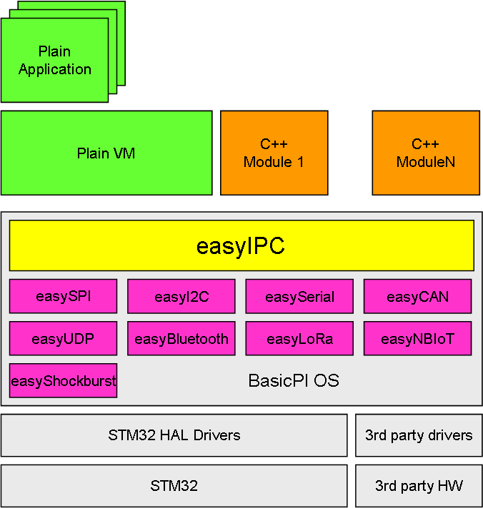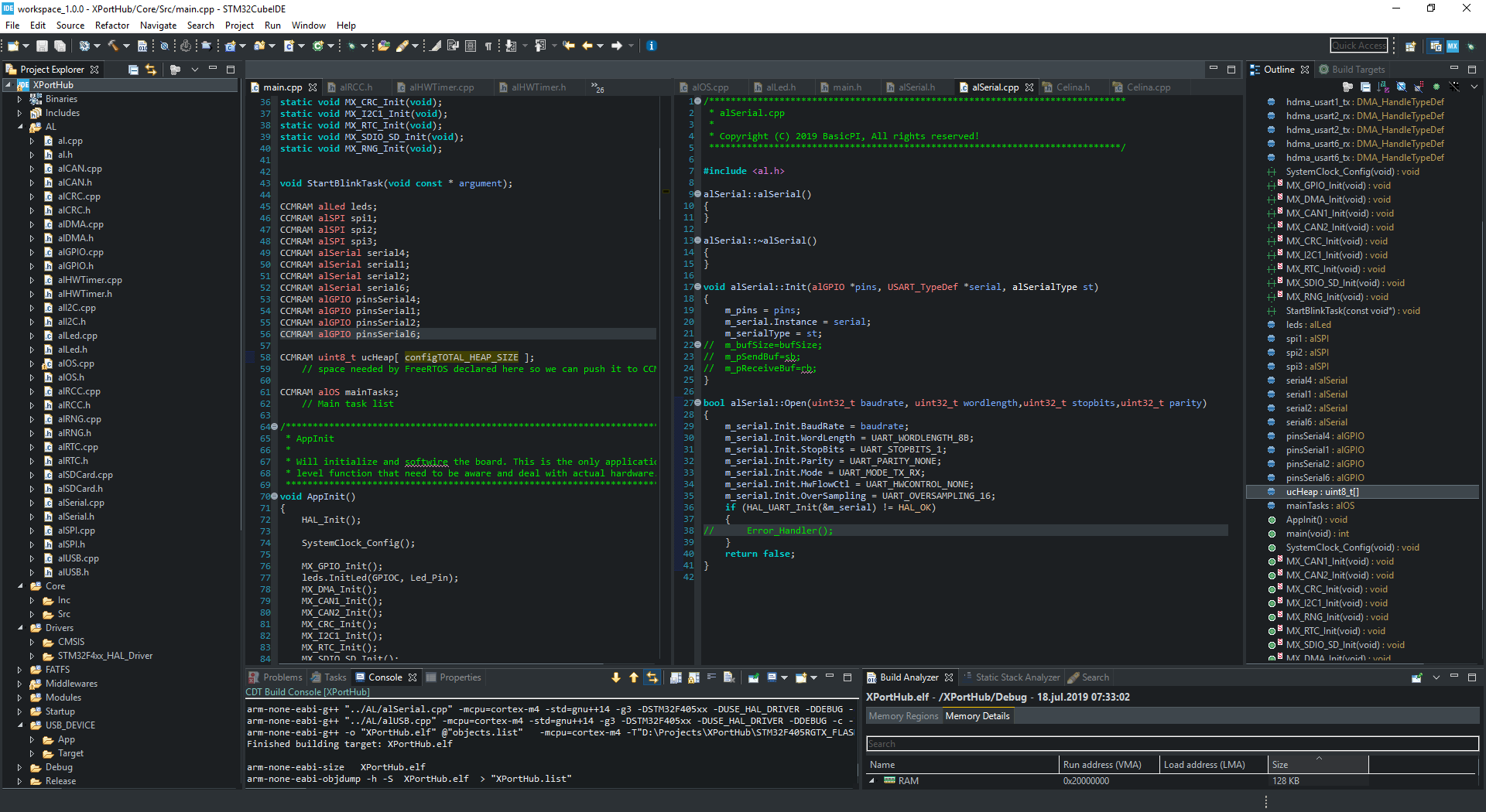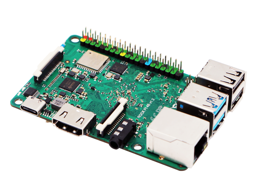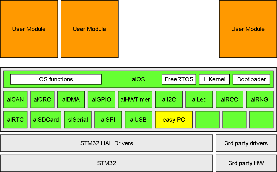
This illustrates the BasicPI Firmware Stack in progress. What I always do in embedded applications is to make a “standard” main.cpp as follows:
- void AppInit()
- {
- // wire hardware
- }
- int main()
- {
- AppInit();
- // start OS
- }
A team I worked in years ago agreed on this standard so we should be able to easy recognize the basic architecture in any application and avoid wasting time figuring out how main() works. How you do this is not as important as the fact that you and your team does it in a systematic way.
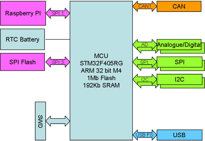
I use C++ so it is very easy to hide all external FW with an abstraction layer. I hide even FreeRTOS because I will replace it later. The modules shown here are just an example, it will be numerous others as I progress. The key is that I want a standard “OS” with known functions so that I can easily move move user modules from Hat to Hat, or make changes to the lower layers without worrying about required SW/FW changes.
Yes, this will bloat a little, but to be honest less that I expected. I use ST HAL drivers for now, but in highly optimized versions and I will remove some of them given time. Right now they are a conveniance.
FreeRTOS should not need any introduction. CubeMX offer installation of FreeRTOS with a single button and I found it easy to install and use + a thread shifter is always handy to have around. FreeRTOS is mature, open source and heavily maintained. The only abstraction I needed here was to hide the functions I needed to use.
L Kernel is a Linear Kernel that exist on top of FreeRTOS. FreeRTOS threads require stack and they can only change as fast as SysTick runs. L Kernel tasks needs no stack and they execute as fast as the MCU is capable of. L Kernel can also run without FreeRTOS and you control that from AppInit(). With no threads you can bit-bang if required and use a alHWTimer (or SysTick) to run a small list of maintenance tasks. L Kernel is also excellent for event driven schemes, buffer handling, software timers etc.
alLed is a funny, new extension – I decided that I use so much time blinking leds that I needed a system to wire it and support blink sequences. This allows an easy path for user apps to signal state through a led.
I threw easyIPC into AL on this drawing, but easyIPC itself is actually an user module, while alEasySPI is a specialized SPI driver. I can’t use alSPI for easySPI because I need to monitor the line for SW signals with very short reaction time. I set the spec to 4 ms, but < 1 ms is realistic. This is the drawback of the SW trick I use + running the SPI on 30+Mbps means it will require some CPU to process. I probably can check faster than 1ms, but that will take a toll on CPU usage. I expect that easySPI will require < 5% CPU usage With 1ms responce times.
I still have not tested Half Duplex SPI and it is busy in real life, and a hot summer with 35 degrees Celsius outside + SW is the largest task on my projects. It is one task that makes you realize how much work that has gone into the word “it is simple” on Arduino.
The upside with nice weather is however that I have to work in my mess of a garden, and my back usually kick in after while forcing me to go inside and sit still – an excellent excuse for working on my projects 
Thanks for Reading!