CH32V307 is a RISC-V based MCU that is created by WCH and that got my attention due to it’s low cost – 3.- USD in quantity 1 and down to 1.9 USD from JLCPCB. I have read about RISC-V as an alternative to ARM for years, but I have not paid much attention to it so far. It exist many MCU’s, but most of them are to expensive to work with for a hobbyist. STM32 and AVR have been the exceptions because MCU’s, tools and toolchains are available at low cost. This does matter because it enables me to use them without the backing of a large company.
WCH should be well known to most hobbyists due to theire CH340 chips.
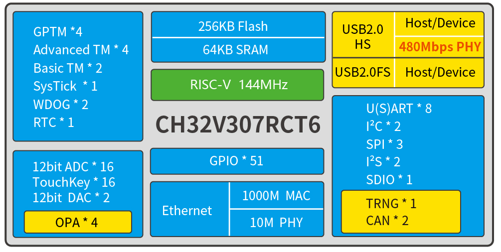
CH32V307 comes in 3 variants – the LQFP64 version is illustrated above and it is a MCU that is comparable to M4 (F4xx and G4xx) series in STM32 as far as performance and functionality goes. I will argue that STM32 is a bit better yet, but it is several aspects of this new MCU that got my attention and made me realize that this might very well be the next dominant MCU.
It cost 1.9 USD in volume of 1000 from JLCPCB – and even quantity 1 is only ca 3.- USD.
A STM32G491Rx cost me ca 12.- USD from Digikey, so a comparable MCU that cost 3.- USD does get my attention – that said STM32G491 only cost ca 9.- USD from PLCPCB, but it is still a 3x in price between MCU’s that seems to be very comparable.
- RISC-V vs ARM
- MoanRiver Studio vs STM32CubeIDE
- Similar speed, Flash, SRAM
- 4 Op amps on both
- FD-CAN on one, Ethernet w/Phy on the other.
- aso
With 4 x OpAmps, 4x Motor Timers, 2xCAN ports, 8xSerial ports, 2xUSB ports, 1xEthernet w/Phy on chip the CH32V307 becomes a very interesting alternative for many applications. But, it is the low cost that is the killer, and makes me realize what an impact this MCU is about to make – assuming it keeps it’s current price/availability.
I don’t expect the eco-structure on CH32V307 to be even close to what I get from STM32CubeIDE yet – but this is an evolving story. This is changing fast!
CH32V307 have a smaller sibbling – still a RISC-V, 48 pins, only 64KB Flash, 32Kb SRAM and 48Mhz, but it cost around 0.4 USD in quantity of 1000 – making it one of the cheapest MCU’s around.
CH32V307VCT6 development board RISC V core support RT Thread onboard| | – AliExpress
Above is the link to a < 7.- USD dev board available – you also need to buy a WCH-Link Debugger – around 10.- USD is all you need to get started with this RISC-V MCU.
