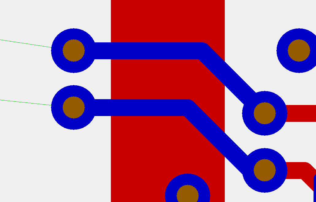
The 2 blue signals crossing the bigger, red Power lane is asking for trouble. The blue lanes are 0-3V ADC signals, while the power lane is feeding PWM MOSFET’s. What will happen is that PWM noise from current spikes will jump over to ADC signals and create a false current signature.
But, I believe it is to my advantage that I have a fast MCU and no electronic filtering, meaning I can apply smart filtering in SW using the high sampling frequencies available on the ADC. Well, we will see. But, I have promissed myself that I will look into 4-layer PCB designers after this one.
