This has been on my list of things to do for a while and represent a few challenges. Chips like AD9851 contains a full DDS that interface to a MCU on one side and give 3.3V signals on the other side. I have yet to decide wherever to use AD9851 or something else, butAD9851 is the candidate as we speak.
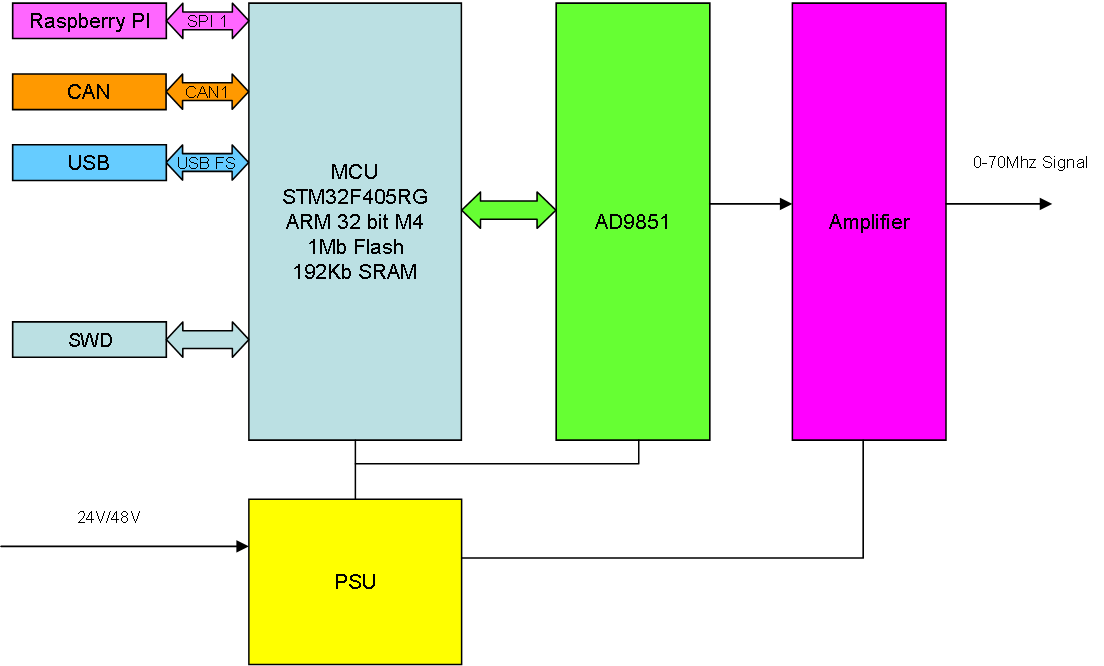
The block diagram above outline the functionality of the DDS. The first part a MCU and AD9851 is straight forward. I have not used AD9851, but I have breakout boards + loads of reference schematics to work on. If nothing else I will make a Hat with 1 x 3.3V out channel. In many cases that is all that is needed and with my capability to stack up Hat’s we already talk about a very nice instrument.
The PSU is straight forward. I use 24 or 48V to create +/- 12 or 24V out as base. The amplifier is however far from straight forward.
First step is to offset the 3.3V signal, the second to amplify it and remember that we talk about signals up to 70Mhz. The Hat might get crowded, so it is possible that I need to split this onto 2 Hats and as such also accept that the amplifier only support 1Mhz or something.
I have dreaded this project a little because I only was on 2 layer designs, but as I now have moved to KiCAD and 4 layers or more is possible I want to give it a go. I think the first step is to make schematics for MCU and AD9851 as well as playing around with my breakout boards a little.
The primary usage for this is test equipment and it’s fun to make your own, but most important fun to have this as a component in my modular system.
