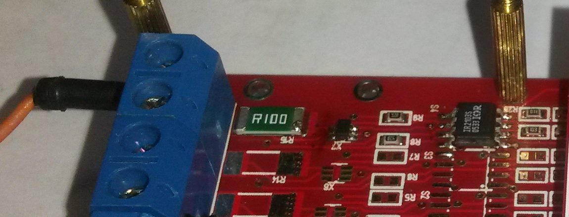
I don’t get much sense out from the INA210 at 0 – 2A. Firstly I realize that I use a far to large Shunt resistor. I use a 0.1R by mistake. 100mA would give 10mV that amplified with 200 should be 2V. At this size the Shunt become my weak point. At 3A it starts getting very warm as I dispose 0,9W and it is rated at 1W. I need to replace this, but I accidentally lack smaller shunt’s yet.
With 15A and 0.001R I should get 0,015V that amplified with 200 should be 3V. With a 12 bit ADC giving a range of 4096 I should in theory have a current sensitivity of ca 4mA (15A / 4096).
For now I need to wait on 0,001 shunts, but I will find a load that can support 0-150mA so I can test this range.
I want to test INA210 a bit more to see if I get any sense out of it, but it cost 50c and the tiny package makes it a pain to use. Using a 2 layer PCB I am also at a disadvantage regarding noise.
As for load testing… I am melting my load at 3A. I use 10 x 0,47Ohn @5W in series to create a 4,7 Ohm 50W resistor, but it get so hot that it melt the soldering tin on my home made load. I have mounted a 40x40x10mm Heat-Sink and the only component getting hot is my 0,1R Shunt. I can manage 10A out from my Lab PSU and that will have to do for now. But, I want to move load testing to a different boards with only PWM driver Circuit before I continue. It is basically so much work to solder a full board that I don’t want to destroy this one. Have been replacing 5 x HEXFET’s so far as I tested without heat-sink. I can only sustain 1A without a heat-sink on. I need to do the math here as I expected more.
All in all – this design seems to work. It will be down to current sensing and finding an optimal heat-sink I think. But, I am currently only testing 3A and it’s a way up to 15A continuously yet – mostly stopped due to lack of test equipment as we speak.
