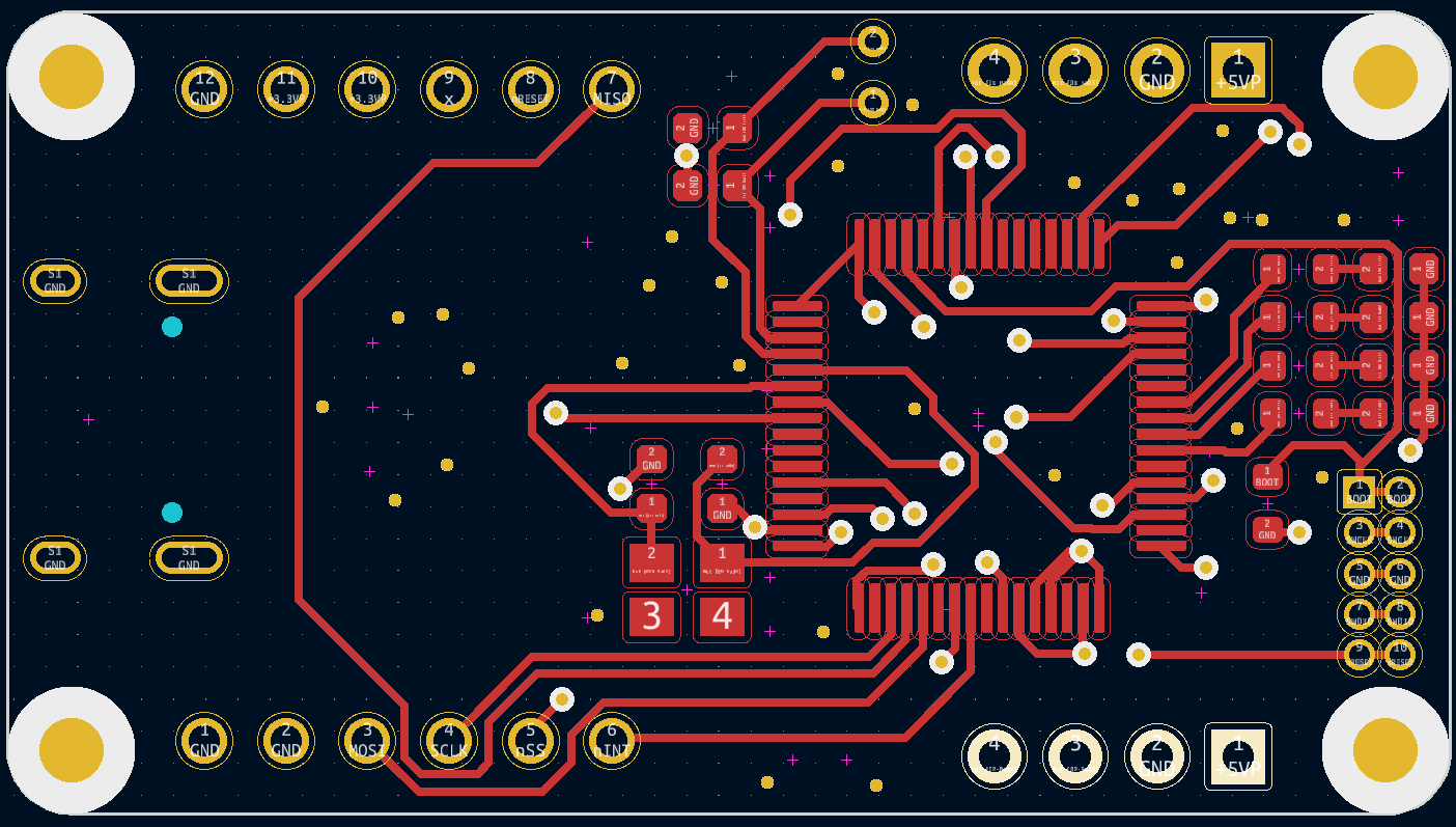
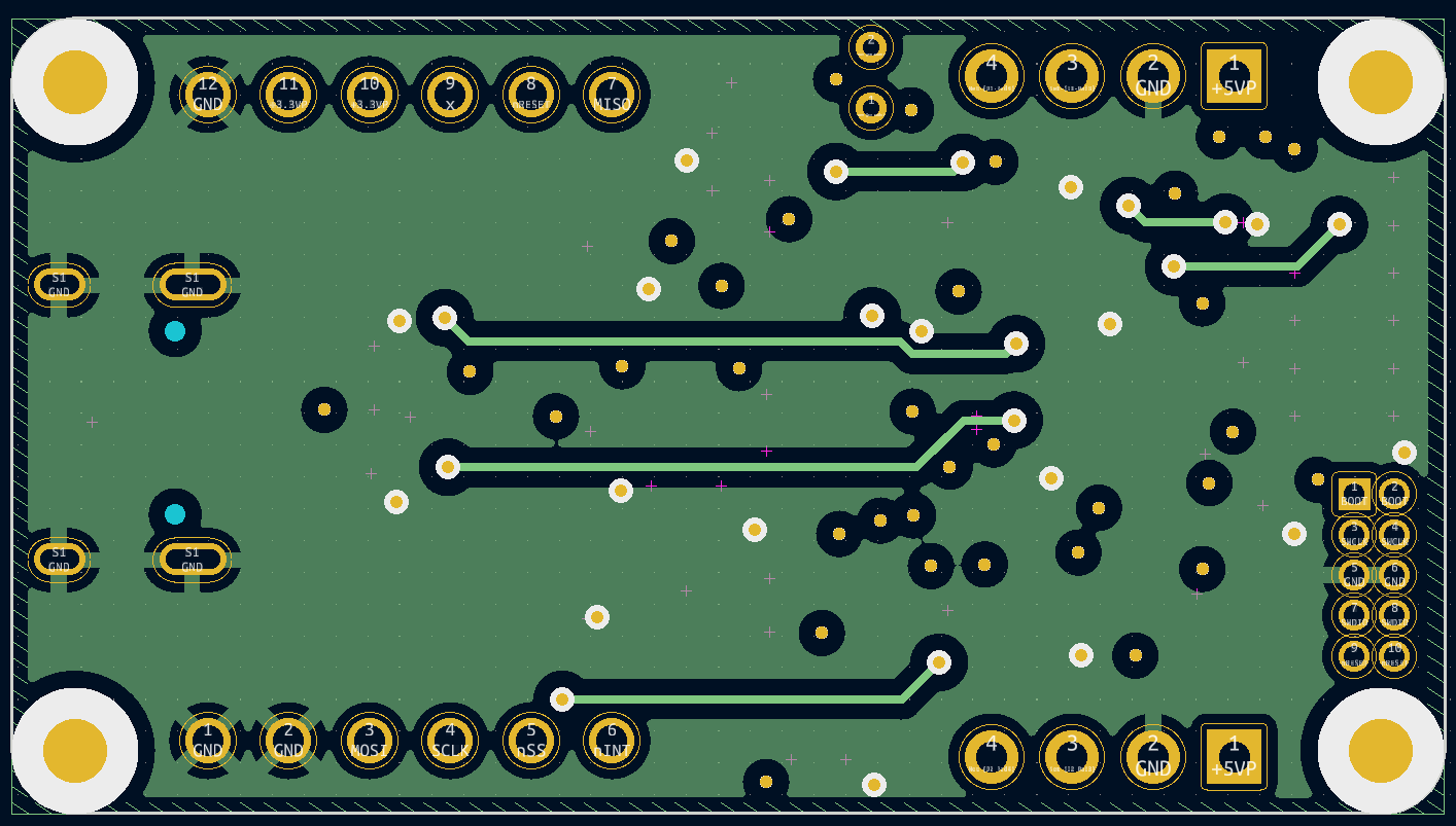
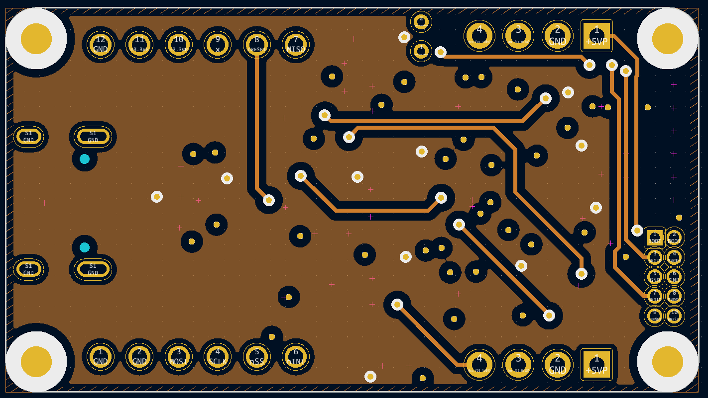
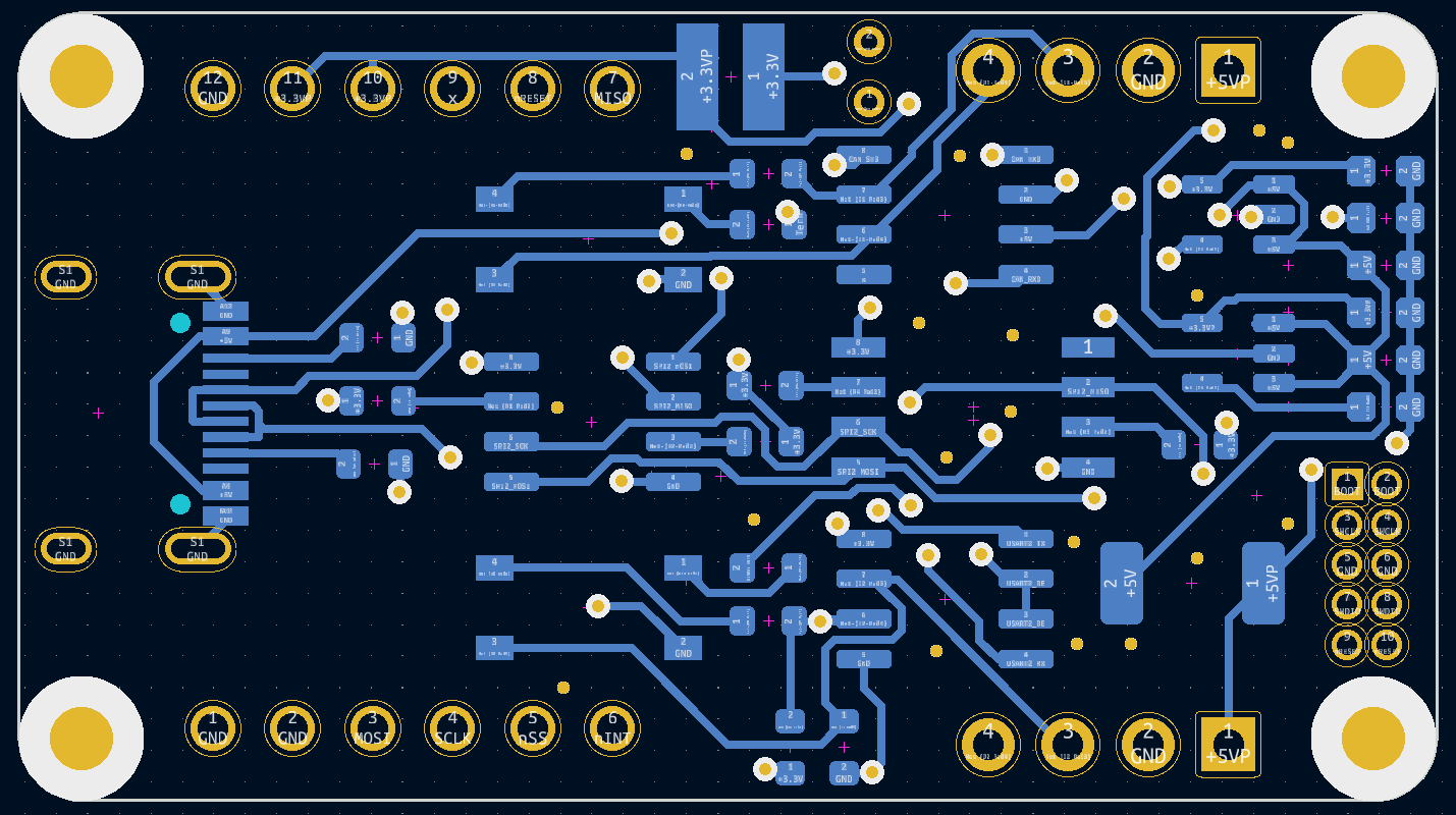
Fisished routing. One days work – first attempt on 4-layer design. I must admit KiCAD did most of the job.
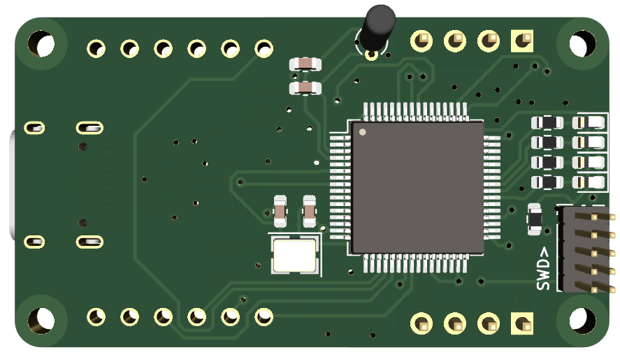
Components top without Ethetnet modul.
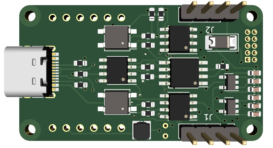
Components bottom layer
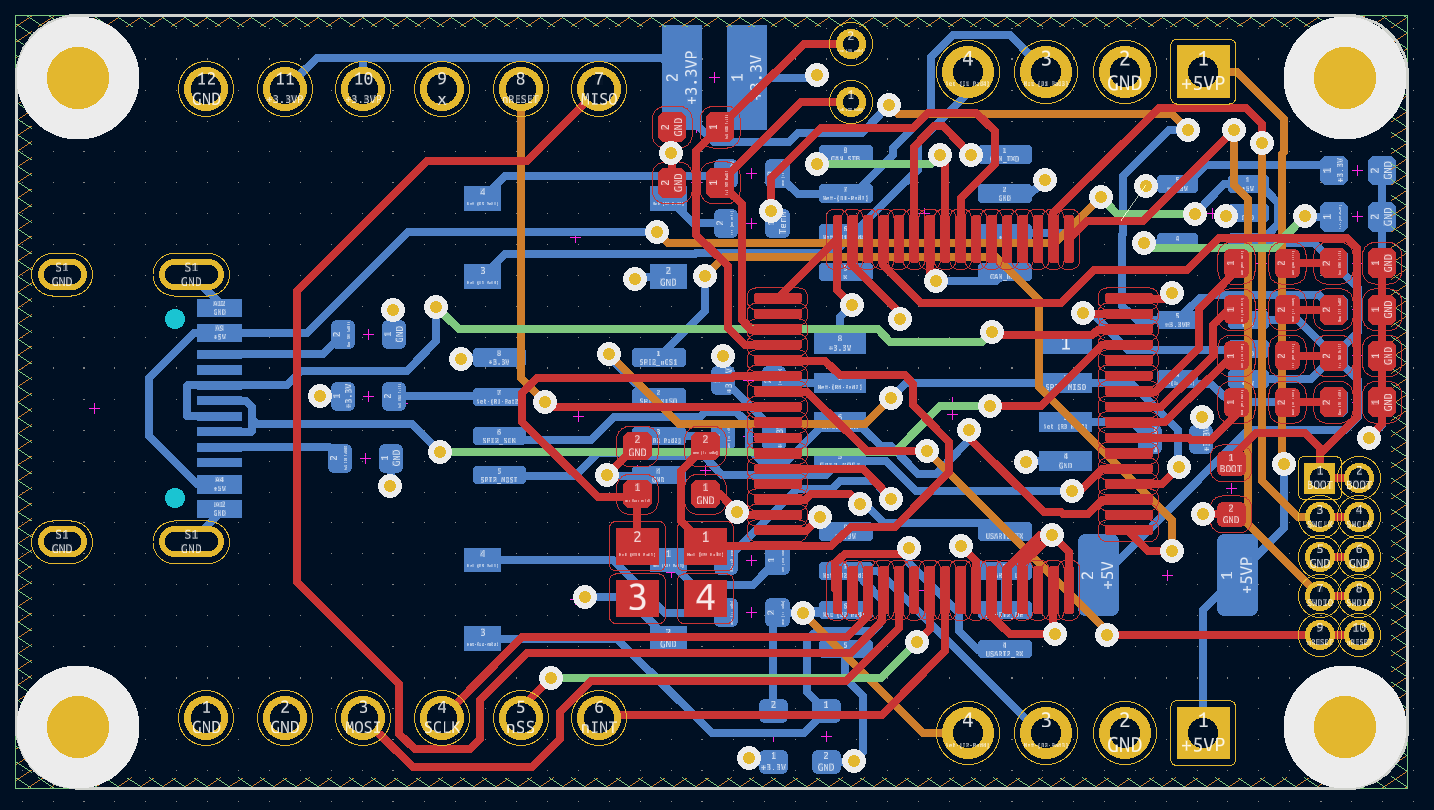
All layers. I decided to use Ground and Power as the middle layers.
I don’t add ground layer on top or bottom since this will be hand-soldiered. Will use 1-2 days to check my work before I order PCB’s.
